Engineering professor co-authors paper on flexographic printing of electronic materials
January 9th, 2017The printing of electronic devices provides inexpensive solutions for diverse applications. But precision on a nanoparticle scale limits the success of sensors and transistors that are electronically printed. Dr. Hossein Sojoudi, Assistant Professor in the Department of Mechanical, Industrial, and Manufacturing Engineering, helped to engineer a solution: nanoporous microstructures that will serve as a next-generation stamp material, comprising polymer-coated aligned carbon nanotubes (CNTs). A paper on this new technology was recently published in Science Advances.
Since its invention in ancient times, relief printing, commonly called flexography, has been used to mass-produce artifacts ranging from decorative graphics to printed media. At present, higher resolution flexography is essential to manufacturing of low-cost, large-area printed electronics. However, due to contact-mediated liquid instabilities and spreading, the resolution of flexographic printing using elastomeric stamps is limited to 50-100 µm. “We designed and engineered the highly porous CNT microstructures to be wetted by colloidal inks, and to transfer a thin layer to a target substrate upon brief mechanical contact. This enabled printing of diverse micron-scale patterns of a variety of functional nanoparticle inks onto both rigid and compliant substrates,” Sojoudi said.
Sojoudi’s role in the research was to develop ultrathin polymer coatings to control elasticity and wettability of the porous CNT microstructures, using initiated chemical vapor deposition (iCVD).
“With a 30 nm thick polymer coating, we were able to prevent aggregation and shrinkage of the porous microstructures,” he said. “In addition to having micrometer-scale resolution, the direct printing of patterns with uniform nanoscale thickness is greatly beneficial to scalable manufacturing of devices such as high-performance transistors and low-cost wireless sensors.”

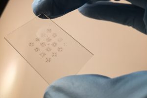
Dr. Sojoudi helped fabricate a stamp made from carbon nanotubes that is able to print electronic inks onto rigid and flexible surfaces. Photo credit: Sanha Kim and Dhanushkodi Mariappan
The project was led by Dr. Sanha Kim, a postdoctoral fellow in Dr. A. John Hart’s research group, in collaboration with other research groups at Massachusetts Institute of Technology. Dr. Sojoudi was part of the research team while conducting his postdoctoral research with Prof. Gareth H. McKinley and Prof. Karen K. Gleason at MIT, before joining UT in August 2016.
This research news has been shared widely. Read more here:
MIT News:
http://news.mit.edu/2016/stamping-technique-printable-electronics-1207
Eurek Alert, The Global Source for Science News:
https://www.eurekalert.org/pub_releases/2016-12/miot-stc120516.php
OOYUZ beta:
http://www.ooyuz.com/geturl?aid=14184497
Sci Feeds:
https://scifeeds.com/news/printable-electronics/
Search for the Good:
http://searchforthegood.com/printable-electronics-mit-news/
Nanotechnology Innovation:


